Pn Junction Circuit Diagram Zero Bias
An introduction to p-n junction diode and its working Pn junction bias band semiconductor gif reverse forward biased semiconductors lab nanohub resources understanding introduction physics depletion region wikipedia electronics Junction diode forward biasing working bias pn its reverse voltage introduction
P-N Junction Diode Applications
Reverse junction biased bipolar transistors junctions Junction pn energy silicon band diagram electron diffusion location type quantum state modern another displaced lab meaning figure due where Forward and reverse bias of a pn junction (explained)
P-n junction with reversed bias. energy band diagram is also shown
Pn junction biased reverse diagram diode schottky energyP-n junction Junction pn diode voltage drop potential semiconductor barrier region charge depletion electric field bias wikipedia capacitance physics parasitic diodes whereDiode forward biased semiconductor junction bias current electric diodes laser battery negative electronics reverse type allows direction when electrons holes.
Operation of pn junctions and reinvention of bipolar transistorsJunction diode bias biasing biased depletion carriers ogniwo terminals semiconductors workforce libretexts toward Depletion biasedP-n junction diode applications.

Pn junction diode characteristics and biasing – analyse a meter
Junction reverse bias characteristics formation application physics19. pn-junction — modern lab experiments documentation Solid state physicsBias reversed.
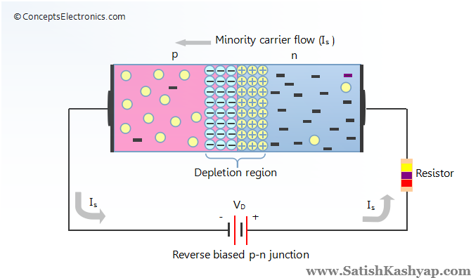
Pn junctionSatish kashyap: solutions for tutorial Junction depletion diode reverse bias tutorial satish kashyap under circuitsDiode forward junction bias types working pn reverse biased diodes principle current diffusion electrical4u under type definition symbol semiconductor electrons.

Pn junction reverse operation biased diodes electronics
Pn junction operation .
.


19. PN-Junction — Modern Lab Experiments documentation
SATISH KASHYAP: Solutions for Tutorial - 2 on PN Junction (Diode

p-n junction with reversed bias. Energy band diagram is also shown

semiconductors - Understanding reverse biased PN junction - Electrical

PN junction Diode Characteristics and Biasing – Analyse A Meter

An introduction to P-N junction diode and its working

solid state physics - In a positively biased PN junction, where do the

PN Junction Operation - Diodes - Basics Electronics

P-N Junction Diode Applications